2
RF Device Data
Freescale Semiconductor, Inc.
MRF6VP11KHR6 MRF6VP11KGSR5
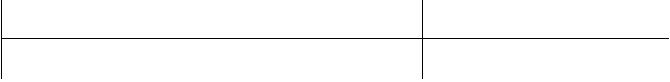
Table 3. ESD Protection Characteristics
Test Methodology
Class
Human Body Model (per JESD22--A114)
2, passes 2000 V
Machine Model (per EIA/JESD22--A115)
A, passes 125 V
Charge Device Model (per JESD22--C101)
IV, passes 2000 V
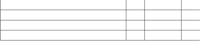
Table 4. Electrical Characteristics
(TA
=25°C unless otherwise noted)
Characteristic
Symbol
Min
Typ
Max
Unit
Off Characteristics
(1)
Gate--Source Leakage Current
(VGS
=5Vdc,VDS
=0Vdc)
IGSS
?
?
10
μAdc
Drain--Source Breakdown Voltage
(ID
= 300 mA, VGS
=0Vdc)
V(BR)DSS
110
?
?
Vdc
Zero Gate Voltage Drain Leakage Current
(VDS
=50Vdc,VGS
=0Vdc)
IDSS
?
?
100
μAdc
Zero Gate Voltage Drain Leakage Current
(VDS
= 100 Vdc, VGS
=0Vdc)
IDSS
?
?
5
mA
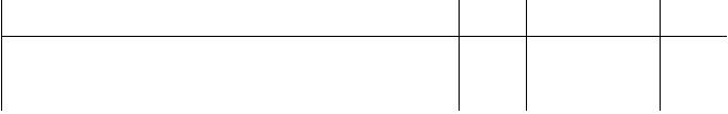
On Characteristics
Gate Threshold Voltage
(1)
(VDS
=10Vdc,ID
= 1600
μAdc)
VGS(th)
1
1.63
3
Vdc
Gate Quiescent Voltage
(2)
(VDD
=50Vdc,ID
= 150 mAdc, Measured in Functional Test)
VGS(Q)
1.5
2.2
3.5
Vdc
Drain--Source On--Voltage
(1)
(VGS
=10Vdc,ID
=4Adc)
VDS(on)
?
0.28
?
Vdc
Dynamic Characteristics
(1)
Reverse Transfer Capacitance
(VDS
=50Vdc±
30 mV(rms)ac @ 1 MHz, VGS
=0Vdc)
Crss
?
3.3
?
pF
Output Capacitance
(VDS
=50Vdc±
30 mV(rms)ac @ 1 MHz, VGS
=0Vdc)
Coss
?
147
?
pF
Input Capacitance
(VDS
=50Vdc,VGS
=0Vdc±
30 mV(rms)ac @ 1 MHz)
Ciss
?
506
?
pF
Functional Tests
(2,3)
(In Freescale Test Fixture, 50 ohm system) VDD
=50Vdc,IDQ
= 150 mA, Pout
= 1000 W Peak (200 W Avg.), f = 130
MHz, 100
μsec Pulse Width, 20% Duty Cycle
Power Gain
Gps
24
26
28
dB
Drain Efficiency
ηD
69
71
?
%
Input Return Loss
IRL
?
-- 1 6
-- 9
dB
1. Each side of device measured separately.
2. Measurements made with device in push--pull configuration.
3. Measurements made with device in straight lead
configuration before any lead forming operation is applied. Lead forming is used for gull
wing (GS) parts.


发布紧急采购,3分钟左右您将得到回复。
相关PDF资料
MRF6VP121KHSR6
MOSFET RF N-CH 50V NI-1230S
MRF6VP21KHR6
MOSFET RF N-CH 1000W NI1230
MRF6VP2600HR6
MOSFET RF N-CH 600W NI1230
MRF6VP3091NBR1
MOSFET RF 50V 350MA TO272-4
MRF6VP3450HR6
MOSFET RF N-CH 450W NI-1230
MRF6VP41KHSR7
MOSFET RF N-CH 1000W NI1230S
MRF7P20040HSR5
MOSFET RF N-CH 40W NI780HS-4
MRF7S15100HR5
MOSFET RF N-CH 28V 23W NI780
相关代理商/技术参数
MRF6VP11KHR6_09
制造商:FREESCALE 制造商全称:Freescale Semiconductor, Inc 功能描述:RF Power Field Effect Transistor N-Channel Enhancement-Mode Lateral MOSFET
MRF6VP121KHR5
制造商:Freescale Semiconductor 功能描述: 制造商:Freescale Semiconductor 功能描述:VHV6 1KW 50V NI1230H - Tape and Reel 制造商:Freescale Semiconductor 功能描述:MOSFET RF N-CH 50V NI1230H 制造商:Freescale Semiconductor 功能描述:RF POWER TRANSISTOR LDMOS
MRF6VP121KHR6
功能描述:射频MOSFET电源晶体管 VHV6 1kW 50V NI1230H RoHS:否 制造商:Freescale Semiconductor 配置:Single 晶体管极性: 频率:1800 MHz to 2000 MHz 增益:27 dB 输出功率:100 W 汲极/源极击穿电压: 漏极连续电流: 闸/源击穿电压: 最大工作温度: 封装 / 箱体:NI-780-4 封装:Tray
MRF6VP121KHSR5
制造商:Freescale Semiconductor 功能描述:VHV6 1KW 50V NI1230HS - Tape and Reel 制造商:Freescale Semiconductor 功能描述:LATERAL N-CHANNEL BROADBAND RF POWER MOSFET, 965-1215 MHZ, 1 - Tape and Reel 制造商:Freescale Semiconductor 功能描述:MOSFET RF N-CH 50V NI1230H 制造商:Freescale Semiconductor 功能描述:RF POWER TRANSISTOR LDMOS
MRF6VP121KHSR6
功能描述:射频MOSFET电源晶体管 VHV6 1kW 50V NI1230HS RoHS:否 制造商:Freescale Semiconductor 配置:Single 晶体管极性: 频率:1800 MHz to 2000 MHz 增益:27 dB 输出功率:100 W 汲极/源极击穿电压: 漏极连续电流: 闸/源击穿电压: 最大工作温度: 封装 / 箱体:NI-780-4 封装:Tray
MRF6VP21KHR5
功能描述:射频MOSFET电源晶体管 VHV6 225MHZ 1000W NI1230 RoHS:否 制造商:Freescale Semiconductor 配置:Single 晶体管极性: 频率:1800 MHz to 2000 MHz 增益:27 dB 输出功率:100 W 汲极/源极击穿电压: 漏极连续电流: 闸/源击穿电压: 最大工作温度: 封装 / 箱体:NI-780-4 封装:Tray
MRF6VP21KHR6
功能描述:射频MOSFET电源晶体管 VHV6 225MHZ 1000W NI1230 RoHS:否 制造商:Freescale Semiconductor 配置:Single 晶体管极性: 频率:1800 MHz to 2000 MHz 增益:27 dB 输出功率:100 W 汲极/源极击穿电压: 漏极连续电流: 闸/源击穿电压: 最大工作温度: 封装 / 箱体:NI-780-4 封装:Tray
MRF6VP21KHR6_10
制造商:FREESCALE 制造商全称:Freescale Semiconductor, Inc 功能描述:RF Power Field Effect Transistor N--Channel Enhancement--Mode Lateral MOSFET
